646e Stm Manipulation and First Principles Simulation of a Molybdenum Disulfide Surface
As the dimensions of CMOS devices continue to scale down, exploring atom based technology for the design and fabrication of logical and electronic devices at the single molecule scale is gaining attention. In this project, we study the possibility to fabricate planar molecular scale devices on an atomically flat surface. To achieve this objective we combine scanning tunneling microscopy (STM) to manipulate and characterize atoms and molecules on a semiconductor surface with first principles simulation of the surface structures and of the STM images. First principles density functional theory calculations are used to determine the surface structures, while STM images are calculated using the one-dimensional scattering formalism with the tight-binding Hamiltonian as implemented in the Elastic-Scattering for Quantum-Chemistry (ESQC) program [1].
Molybdenum disulfide (MoS2) was selected as a potential substrate to fabricate the atomic scale device. MoS2 is layer-structured semiconductor with an indirect band gap of 1.2 eV, similar to that of silicon (1.1 eV). Due to its layered structure and two-element composition, MoS2 exhibits some very interesting electrical and chemical properties. For example, the sulfur surface is chemically inactive. In addition, experimental studies indicate that it is possible to remove single sulfur atoms using the STM tip [2], and it can be envisioned that atomic lines can be created by removing sulfur atoms from the MoS2 surface. Alternatively, metal islands deposited on the MoS2 surface might be used as the electrodes of a molecular device.
A number of experiments and simulations will be reported to highlight the prospects of using MoS2. First the possibility of removing single sulfur atoms from the MoS2 surface using a voltage pulse from the STM tip was studied using first principles calculations. The DFT calculations quantify the effect of the electric field between the MoS2 surface and a W tip on the activation energy required to extract a sulfur atom from the MoS2 surface (Figure 1). Calculated STM images for a surface with S vacancies were compared with experimental images.
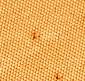
In a second experiment, it was found that the MoS2 surface undergoes a transformation upon heating to 1000 K in vacuum. STM images of the MoS2 surface before and after the thermal treatment show a clear change in the atomic structure (Figure 2). DFT calculations indicate that some surface S atoms can evaporate in vacuum at 1000 K, forming a surface with double sulfur rows (Figure 3). STM image calculations indicate that the bright lines in Figure 2b correspond to the sulfur atom lines. We are currently studying the properties of the sulfur double lines. Initial Density of States calculations indicate they might behave as atomic wires.
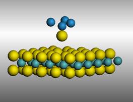
Figure 1. Model used to study sulfur atom transfer between the MoS2 surface and the W tip
 аааааа
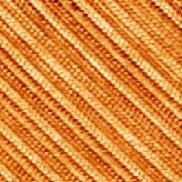
(a)ааааааааааааааааааааааа ааааааааааааа ааааааааааааа ааааааааааааа аааааа (b)
Figure 2. (a) STM image of the pristine MoS2 (0001) surface; (b) STM image of the MoS2 surface after thermal treatment.
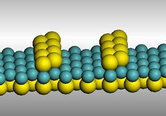
Figure 3. Proposed structure for the reconstructed MoS2 surface
References:
[1]а P. Sautet, C. Joachim, Phys.Rev.B 1988, 38, 12238
[2]а S. Hosoki, S. Hosaka, T. Hasegawa, Appl. Surf. Science, 1992, 60/61, 643